Better way found to determine the integrity of metals
Better way found to determine the integrity of metals
Researchers at the University of Waterloo have found a better way to identify atomic structures, an essential step in improving materials selection in the aviation, construction and automotive industries.

Article from University of Waterloo
Researchers at the University of Waterloo have found a better way to identify atomic structures, an essential step in improving materials selection in the aviation, construction and automotive industries.
The findings of the study could result in greater confidence when determining the integrity of metals.
Devinder Kumar, a PhD candidate in systems design engineering at Waterloo, collaborated with the Fritz Haber Institute (FHI) in Berlin, to develop a powerful AI model that can accurately detect different atomic structures in metallic materials. The system can find imperfections in the metal that were previously undetectable.
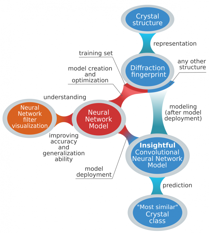
The model workflow of automatic crystal structure classification. First, every crystal structure is represented by the two-dimensional diffraction fingerprint. Then, a small subset of these structures are used as training set to generate a classification model. In particular, a convolutional neural network is used, and optimized minimizing the training set classification error. However, this is in general not enough to have a sound and generalizable model. Thus, we unfold the neural network internal operations by visualization, and ensure that the model arrives at its classification decision on physically motivated grounds. Finally, a classification model is deployed, and crystal structures can be directly and efficiently classified without any additional model optimization.
"Anywhere you have metals you want to know the consistency, and that can't be done in current practical scenarios because current methods fail to identify the symmetry in imperfect conditions," said Kumar, who is a member of the Vision and Image Processing Research Group under the supervision of Alexander Wong, a professor at Waterloo and Canada Research Chair in the area of artificial intelligence. "So, this new method of evaluating metallic material will lead to better material design overall and has the potential to affect all the industries where you need material designing properties."
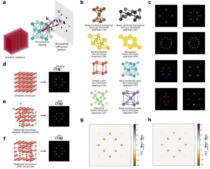
The two-dimensional diffraction fingerprint. a Schematic representation of the two-dimensional diffraction fingerprint calculation. An incident plane wave is scattered by the material, and the diffraction pattern on a plane perpendicular to the incident radiation is computed. b Prototypes of the crystal classes considered in this work. c Examples of two-dimensional diffraction patterns for materials belonging to each of the eight classes. The ordering is the same as b. Rhombohedral and hexagonal structures have the same two-dimensional diffraction fingerprint. d–f A pristine simple cubic structure (d), the same structure with 25% of vacancies (e), and with atoms displaced randomly according to a Gaussian distribution with standard deviation of 0.08 Å (f), together with their diffraction fingerprints. g, h Difference between the diffraction fingerprints of the defective (e), (f) and the pristine structure (d).
FHI came up with a new scenario that can artificially create data, which relates to the real world. Kumar along with his collaborators was able to use this to generate about 80,000 images of the different kind of defects and displacements to produce a very effective AI model to identify various types of crystal structures in practical scenarios. This data has been released to the public so people can actually learn their own algorithms.

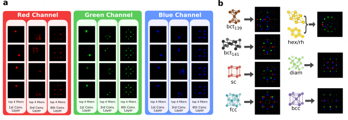
Schematic representation of the convolutional neural network (ConvNet) used for crystals classification. a A learnable filter (also called kernel) is convolved across the image, and the scalar product between the filter and the input at every position is computed. This results in a two-dimensional activation map (in red) of that filter at each spatial position, which is then passed through a rectified linear unit (ReLu)66. b The same procedure as point a is applied to this activation map (instead of the original image), producing another activation map (in purple). c A downsampling operation (in blue) is performed to coarse grain the representation. Six convolutional and two downsampling (max pooling) layers are stacked sequentially (see Methods for additional details). d The output of the convolutional/downsampling layers sequence is passed to fully connected layers (regularized using dropout67) to complete the classification procedure. e The ConvNet outputs the probabilities that the input image, and therefore the corresponding material, belongs to a given class. Minimizing the classification error, the above-mentioned filters are learned—through backpropagation68—and they will activate when a similar feature (e.g., edges or curves for initial layers, and more complex motifs for deeper layers) appears in the input.
"In theory, all metallic materials have perfect symmetry, and all the items are in the correct place, but in practice because of various reasons such as cheap manufacturing there are defects," Kumar said. "All these current methods fail when they try to match actual ideal structures, most of them fail when there is even one per cent defect."
"We have made an AI-based algorithm or model that can classify these kinds of symmetries even up to 40 per cent of defect."
Neural network predictions on structural transitions. a, b Body-centered-cubic (bcc) to simple cubic (sc) structural transition. a Examples of a bcc, an intermediate bcc/sc, and a sc structure. b Distributions of classification probability for the bcc (purple) and sc (red) classes as a function of the percentage of central atoms being removed (see text for more details). The shaded area corresponds to a range of one standard deviation above and below these distributions. c, d Structural transition: transition path including rhombohedral, body-centered cubic, simple cubic and face-centered cubic structures. The prototypes are generated using the AFLOW Library of Crystallographic Prototypes49 .
The study, Insightful classification of crystal structures using deep learning, was published recently in the journal Nature Communications.


