NSI Laser opens applications lab
NSI Laser opens applications lab
NSI Laser, Fremont, Calif., in April opened a new applications laboratory (App Lab) intended to meet the rising demand for new and advanced laser micromachining processes. The App Lab is a direct "response to the whole electronics industry moving toward high density interconnect (HDI) and finer geometry PCBs," according to a company news release.n
NSI Laser, Fremont, Calif., in April opened a new applications laboratory (App Lab) intended to meet the rising demand for new and advanced laser micromachining processes. The App Lab is a direct "response to the whole electronics industry moving toward high density interconnect (HDI) and finer geometry PCBs," according to a company news release.
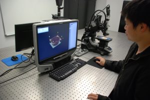
The lab is equipped with NSI's unique dual-head laser systems to meet these new demands. It also features analytical capabilities such as 3D imaging for real time sample process evaluation.
The App Lab will be managed by Dr. Yung Kuo, who recently joined NSI Laser as its Senior Laser Applications Engineer. Yung brings over 25 years of practical laser micromachining experience and process development.
"We are delighted to launch our App Lab to better serve our prospective customers," said Dr. Kuo. "With micro vias becoming less than 5 mils, conventional PCB processes no longer apply; and laser micromachining is the only option. We are ready to assist our customers in this new process development."
For more information, visit the App Lab web page on the NSI Laser website.